My 8-bit breadboard computer
Table of Contents
The idea of building a simple 8-bit computer from scratch first crossed my mind during a computer architecture course at university. While studying with a friend, we were amazed to see how even a basic computer could be constructed using simple, discrete components. In the end, it's all about having enough NAND gates, right?
My friend Federico had just finished his PCB-based 8-bit computer, which gave me the push to try something similar. But instead of learning how to design a PCB with KiCad, I decided to use a breadboard.
In this article, I'll walk through my 8-bit breadboard computer and focus on the lessons I learned—especially for anyone thinking about embarking on a similar project.
The 8-bit computer
The computer design is based on the excellent course by Ben Eater. On his website, he has also provided the schematics for the computer. This computer is an implementation of the Simple-As-Possible (SAP) computer model, which is described in the book Digital Computer Electronics by Malvino and Brown.
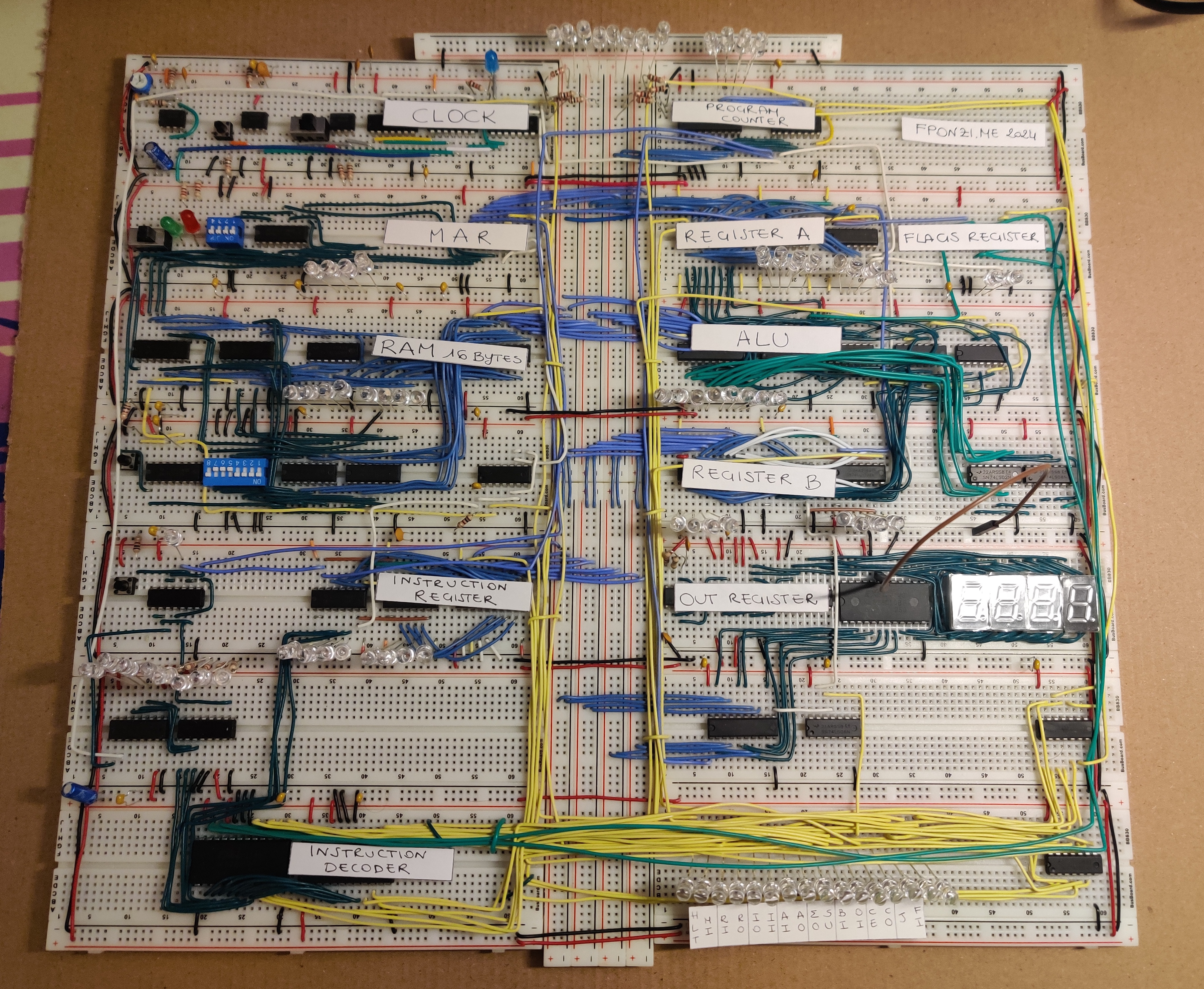
Here is the schematic of the computer:
Here are the specs:
- 8-bit BUS
- 2 registers
- ALU capable of adding and subtracting 8-bit 2's complement integers from registers A and B
- 4-bit addressable RAM, providing 16 bytes of RAM shared between code and data
- Adjustable clock speed up to 200 Hz
- 3-digit signed digital display
If you're wondering why it only has 16 bytes of RAM, it's because inputting a program is a manual process—you need to insert each instruction into every memory slot by hand. Since there's currently no way to store or load programs from persistent storage, this process becomes laborious.
On average, it takes about 15-20 seconds to manually load a single instruction, so loading a larger program can take around 5 minutes. Adding more RAM would be useful if I also implemented a way to store and load programs. Although this isn't part of the initial design, people have already shared instructions on how to implement it.
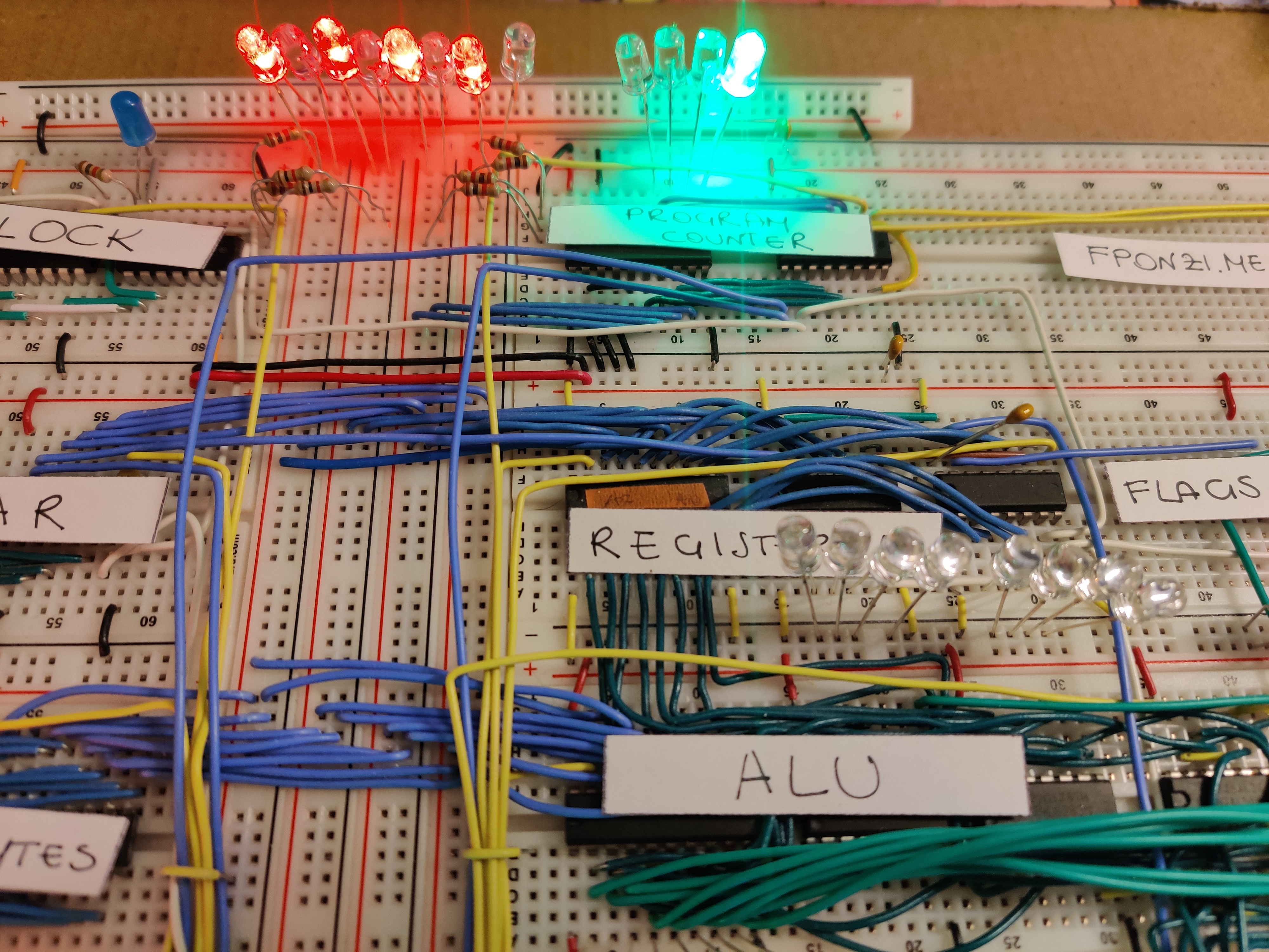
Modules and a Simple Instruction
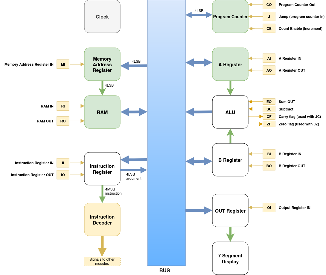
The Program Counter (PC) is a register that holds the address of the current instruction. When the computer starts, it is set to zero and increments with each executed instruction.
The Bus works like a shared buffer. Different components communicate by writing to and reading from the bus at the right time. It consists of 8 lines, one per bit, that interconnect the various modules.
The Memory Address Register (MAR) reads the address of the next instruction to load, and the RAM, composed by two 4x16 bit RAM chips, writes the content to the Bus.
The Instruction Register picks up the instruction next. Like the A and B registers, the Instruction Register is a D flip-flop that interfaces with the bus via a tri-state buffer. This buffer decouples register read/write operations from the bus.
The Instruction Decoder then steps in. It has its own local Program Counter to count microinstructions. Each instruction is mapped to 3 microinstructions, each taking one clock cycle to complete. The mapping is computed using a ROM, which acts like a persistent hashmap.
Each microinstruction coordinates the reading and writing from the Bus.
An ADD instruction looks like this: ADD <address>. It adds the content pointed to by the address to Register A. These are the steps:
- First clock cycle:
- Signals Enabled: Memory In and Instruction Out.
- Instruction Out allows the Instruction Register to write the address argument to the Bus, and Memory In enables the MAR to read from the Bus.
- Second clock cycle:
- Signals Enabled: RAM Out and Register B In.
- RAM Out writes the content pointed to by the RAM (since the MAR is pointing to
<address>) into Register B.
- Third clock cycle:
- Signals Enabled: Register A In and Sum Out.
- Sum Out writes the result of the ALU to the Bus, and Register A In stores the Bus's content into Register A.
And there you have it! Now Register A contains A + <address>.
The ALU consists of two 4-bit adders that continuously sum the contents of the A and B registers. A tri-state buffer coordinates writing to the Bus. The ALU also stores the result in the Flags Register, indicating if the last operation resulted in a carry bit or a zero, which are used for conditional jumps.
We can use the Output Register and the 7-Segment Display to show the content of Register A. A ROM maps numbers to the segments that need to light up to display the correct number.
Everything is driven by the Clock, which uses the famous 555-timer in three modes: astable, bistable, and monostable. These modes let you advance the clock automatically and adjust the speed with a knob, or switch to a step mode, allowing you to step through the code like a debugger.
Assembling
One of the great things about the SAP architecture is its modularity. This made it possible to assemble (and especially test) the computer module by module. Initially, I was cutting wires with a wire cutter, but I eventually upgraded my tools by getting a wire stripper and some good tweezers, which made the overall experience much more pleasant. Still, there were a lot of wires to connect, and I can't imagine building a computer with more than 8 bits this way!
In this section, I'll share some of the lessons I learned while assembling the computer.
Color coding the wires
Something that might seem irrelevant at first but becomes crucial later is color-coding all the wires. For example, using black for ground and red for VCC. If I see a black wire connected to power, I immediately know something is wrong. Similarly, by consistently using white for the clock signal, it's much easier to trace its path through the computer and its various components.
It's important to note that some wire kits, like this one:
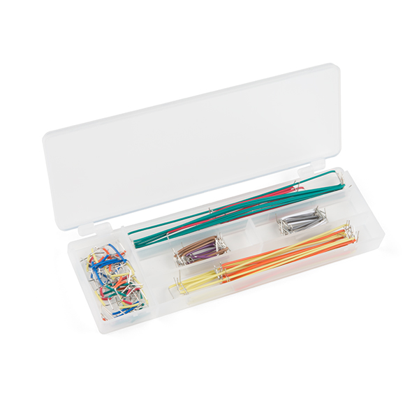
are color-coded by length. I'd discourage using them and recommend cutting wires as needed.
Wiring and layering
PCBs have multiple layers, but on a breadboard, there's only one surface. To solve intersections, you can layer wires on top of each other. In some parts of the computer, I ended up with as many as four layers of wires. The wire's gauge, measured by AWG (American Wire Gauge), is also important. If the wire is too thin, it might not provide good power distribution. On the other hand, if it's too thick, it becomes harder to manage.
Cutting wires can also be tricky because, ideally, you want to cut the shortest possible wires to connect two points. However, there are a couple of issues with this approach:
- If you miscount the holes or misplace a chip, you'll need to cut a new wire.
- Even if the chips are correctly placed, if the wire is too short, it becomes difficult to move components or reroute wires underneath it (due to wire layering).
To make everything neat, I'd need to rebuild the computer from scratch, now that I know how it all fits together. This aligns with the adage "make it work, then make it pretty." For example, I would have added power strips across the board right from the start, but doing it later made fitting the wires much harder.
LEDs and resistors
In his videos, Ben Eater often plugs in LEDs as needed to check the outputs of chips. However, if you look at the schematics, every time an LED is used, it is placed in series with a 300Ω resistor. This adds complexity to the breadboard computer, and I've seen three common solutions to manage it:
- Refactor the layout to fit both LEDs and resistors.
- Connect/solder the LED and resistor into a single component to save space.
- Use LEDs with integrated resistors.
While I initially used option 2, by the end of the project, I switched to option 3. This made the setup look cleaner and saved time when connecting LEDs and resistors.

I was connecting them rather than soldering because I felt it was more time efficient. There are about 70~ LEDs across the entire computer, with even more used during debugging.
Connecting LEDs directly to the chip outputs, as Ben does in his videos, can be risky if you're not using the same chips. The LEDs will draw current from the chip outputs, which could potentially damage the chips if they aren't designed to handle that current.
Pull up, pull down and connecting things
Initially, I thought inputs in a circuit could only have two states: high or low (1 or 0). However, there's a third state known as "floating" state, when the input is not connected to anything. Why wouldn't you want to connect all the pins?
Let's take an AND gate chip, such as the SN74LS08N, as an example:
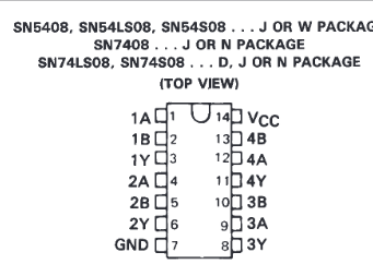
The output 1Y is the result of 1A AND 1B. If you only need two outputs, you don't need to connect inputs 3A/3B or 4A/4B. But what happens if 1A is connected to HIGH and 1B is left floating? It depends on the chip.
The chips in this build use internal pull-up resistors, meaning they default to a HIGH (TRUE) state when the pin is floating. In the previous example, if 1A is connected to HIGH, the output 1Y will follow the state of 1A, as the chip assumes 1B is also HIGH by default.
This can cause issues if not accounted for. For instance, let's say 1B is connected to a button, and I want 1Y to be HIGH only when the button is pressed.
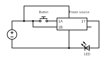
Now, even when the button is not pressed, 1Y will always be active. In this case, adding a pull-down resistor ensures that when the button is not pressed, the input is tied to ground, leading to the desired behavior: the LED only lights up when the button is pressed.
Debugging
After connecting the modules through the bus and linking the control logic, the computer didn't work right away, as expected. Debugging this was similar to software debugging in some ways, but electricity can't be abstracted away.
Make your assumptions
Debugging the computer is like any other investigation: you form assumptions, develop a hypothesis, and dive in. A common assumption might be that the chips are functioning according to their logic (e.g., an AND chip will output 1 only if both inputs are 1). Another assumption is that the wires are connected correctly. Miswiring was one of the most frequent issues I encountered, so I would always start by carefully double-checking the wiring. Sometimes, while refactoring wires, I would accidentally misconnect them. In any case, if you haven't checked the wiring, you can't assume it's correct. With multiple wire layers, it becomes surprisingly difficult to trace connections. The multimeter's continuity test, which checks for proper connections, was vital for troubleshooting.
Check Your IC Pins
Another problem I encountered was related to the pins (legs) of the ROM chip. This little component wasted a few hours of my time as I tried to debug both my code and the ROM programmer:
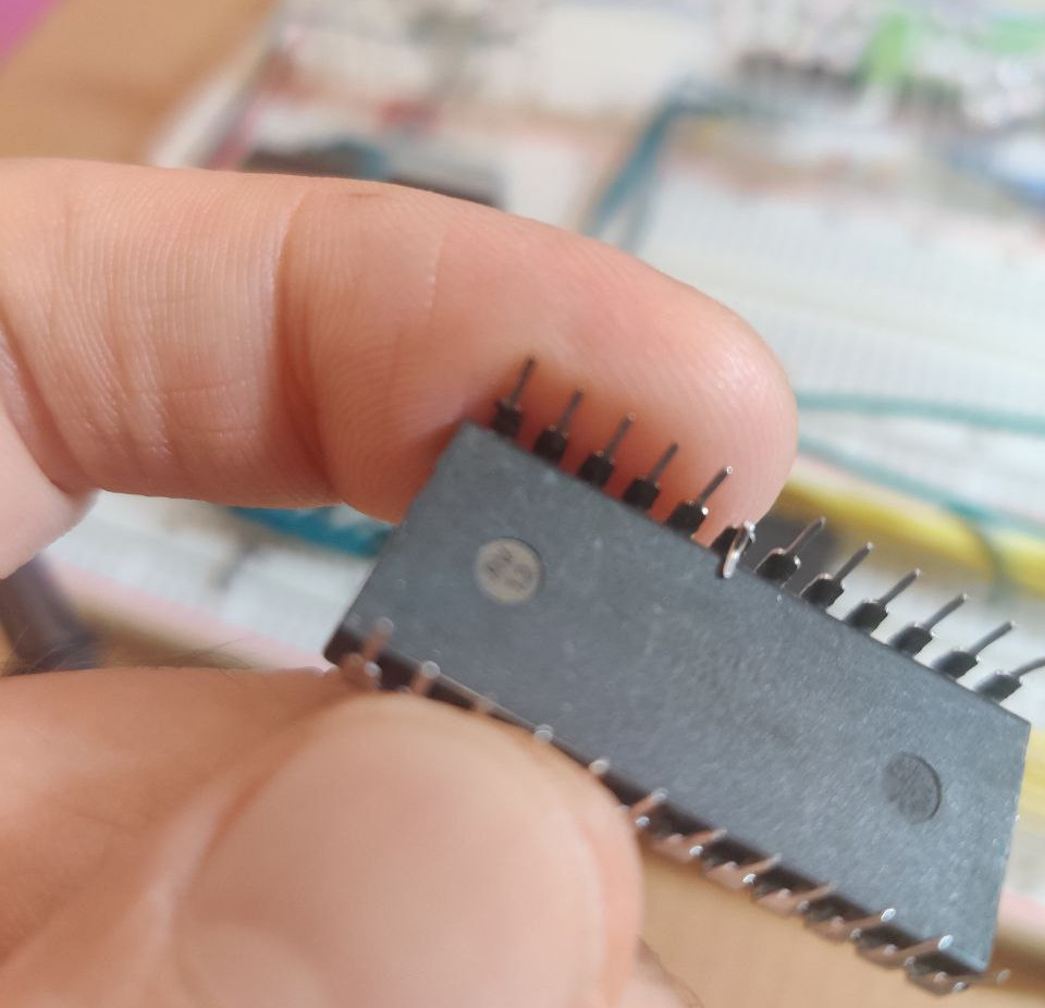
When troubleshooting leads you to suspect the chip itself, isolating and testing it can be helpful for diagnosing malfunctions.
Using patterns for debugging
A clever trick I learned from Ben Eater is to use patterns for quick diagnostics. For example, I noticed that when loading a value from the bus into register B, a bad value was being loaded. The instruction LDI 10101010, which should result in LEDs alternately turning on and off, gave me a quick visual cue:
Pattern on the bus:
10101010 → LEDs alternate between on and off.
However, when loaded into the B register, I observed:
Pattern loaded in the register:
01100110
It became quickly clear that I had either swapped the input or output wires, in pairs.
Broken by design
Even after wiring everything correctly, I couldn't get the system to work properly. Fortunately, the r/beneater subreddit is quite active, and I found helpful troubleshooting steps there. A pinned post highlights the common experience:
- Even if you follow Ben's videos exactly, it is almost guaranteed that your computer will not work as expected.
- Because the computer won't work by just following Ben's videos, you need to be someone who is willing to spend some time on Reddit, YouTube, and Google searching for solutions to the various problems that you will inevitably encounter.
In my case, among other things, I found, for example, that I had 1.4V constant on some bus lines, causing incorrect reads of 1s. To make matters worse, 1.4V wasn't enough to light the LEDs, so I initially thought the value was 0. This was discussed in a Reddit post, and the fix was to replace the pull-down resistors on the bus from 10kΩ to 1kΩ resistors.
Sometimes, assumptions are broken
I spent a lot of time with my multimeter trying to figure out why certain LEDs were turning on when they should have been off. One particular issue stemmed from a broken hex inverter, the SN74LS04N. This chip performs the NOT operation and is part of the control logic. According to the datasheet, it should invert the input signal. However, when I measured an output for a 0 input, I was getting around 4.3V. Even when the input was 4.3V, the output stayed the same—clearly not working.
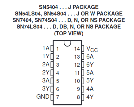
| Function Table (Each Inverter) | |
|---|---|
| Input A | Output Y |
| High | Low |
| Low | High |
After removing the chip and testing it in isolation on another breadboard, I confirmed it was faulty. I compared it to a functioning SN74LS04N, which behaved correctly. In the end, I had to order a replacement chip. During this troubleshooting, I also discovered that my secondary breadboard was faulty, which further complicated debugging.
Power is important
Power distribution is one of the biggest challenges for a breadboard computer. Breadboards have high impedance, which limits how well power is distributed, and they also suffer from parasitic capacitance, which can cause signal loss or noise at high frequencies. To counteract these issues, decoupling capacitors can be used to stabilize the power supply. Ben Eater addresses these concerns in one of his videos, discussing the importance of using a good-quality breadboard and proper power management techniques. I made mistakes when adding some connections, so I didn't need extra problems caused by a low-quality breadboard.
As mentioned in the assembly section, I wish I had interconnected the middle boards earlier to improve power distribution. Using SN74LS series chips (like the SN74LS173AN D-flip-flop), the minimum operating voltage is 4.75V. With a 5V input and many LEDs, it can be tricky to maintain a voltage above this threshold throughout the board.
After various tests, I found that connecting power in the center of the board provided the best distribution, with voltage levels remaining above 4.8V across all components.
As for power consumption, I measured around 810mA with all LEDs on, which is well within the 2A limit of the charger I'm using.
Programming
Let's get to business! How to program this computer?
The process looks like this:
- Write a high level version of the program using pseudocode.
- Translate the pseudocode into assembly.
- Translate assembly to machine code.
- Power on the PC with the clock paused and MAR switched to programmer mode..
- For each instruction/data: select an address, write the 8-bits values, and load them by clicking the button.
- Turn MAR to running mode and start the clock.
The first few steps could be automated by writing an assembler, but I haven't checked if anyone has already implemented it. The last few steps (which are the most time-consuming and also error-prone) could be avoided by using a more high-level interface, like Arduino, but that requires changes to the design.
As an example of how it feels like use this computer, let's try to write a Fibonacci counter!
As a reminder, the n-th Fibonacci number is defined as:
$$ fib(n)=fib(n-1) + fib(n-2) $$
So the first 14 numbers are: 0, 1, 1, 2, 3, 5, 8, 13, 21, 34, 55, 89, 144, 233.
If you want to give it a try and write it yourself, pause here. Below is the list of supported instructions:
| Instruction | Code | Description |
|---|---|---|
| NOP | 0000 | No-op. |
| LDA | 0001 | Load the content of the input address to register A. |
| ADD | 0010 | Loads the content of the address to register B and sums it to the content of register A. |
| SUB | 0011 | Same as above but for subtraction. |
| STA | 0100 | Store content of register A to the input address. |
| LDI | 0101 | Load Immediate the value to register A. |
| JMP | 0110 | Jump unconditionally to the input address. |
| JC | 0111 | Jumps if the adder last operation had a carry. |
| JZ | 1000 | Jumps if the adder last operation was zero. |
| OUT | 1110 | Outputs the contents of A to the 7 segment display |
| HLT | 1111 | Halts the clock and with that the execution of the program and the computer. |
Remember, there are only 16 bytes for both instructions and data. Ben also has a nice video about this exercise, so I would recommend watching it if you're curious.
Let's start by writing a high-level version of the program using pseudocode.
This is the program:
int main() {
  while (true) {
       int z = 0;
       int x = 0;
       int y = 1;

       do {
           printf("%d\n", x);
           z = x + y;
           x = y;
           y = z;
       } while (x < 2<<7);
	}
}
This simple program will iteratively print all the Fibonacci numbers up to the maximum allowed value and then restart from the beginning.
Now that we have a program, we can manually transform it into assembly using the supported instructions. Each assembly instruction can then be converted to machine code:
Instructions:
| Index | Binary index | Instruction | Machine Code |
|---|---|---|---|
| 0 | 0000 | LDI 1 | 0101 0001 |
| 1 | 0001 | STA 14 | 0100 1110 |
| 2 | 0010 | LDI 0 | 0101 0000 |
| 3 | 0011 | OUT | 1110 0000 |
| 4 | 0100 | ADD 14 | 0010 1110 |
| 5 | 0101 | STA 15 | 0100 1111 |
| 6 | 0110 | LDA 14 | 0001 1110 |
| 7 | 0111 | STA 13 | 0100 1101 |
| 8 | 1000 | LDA 15 | 0001 1111 |
| 9 | 1001 | STA 14 | 0100 1110 |
| 10 | 1010 | LDA 13 | 0001 1101 |
| 11 | 1011 | JC 0 | 0111 0000 |
| 12 | 1100 | JMP 3 | 0110 0011 |
Data:
| Index | Binary Index | Variable |
|---|---|---|
| 13 | 1101 | x |
| 14 | 1110 | y |
| 15 | 1111 | z |
The first 4 bits are used to identify the instruction, and the next 4 bits are for the arguments. For example, to translate STA 14:
- The
STAoperation has the instruction code0100. - The number 14 in binary is
1110. - Therefore,
STA 14becomes0100 1110.
The instruction codes were decided when programming the instruction decoder. More instructions could be added as long as we have free indexes available.
Coming back to the translation, it uses the entirety of the available 16 bytes! Phew, that was close. Now that we have the program, we need to test it out.
In this video, I'll show parts 4 to 6 of the list above:
- Power on the PC with the clock paused and MAR switched to programmer mode.
- For each instruction/data: select an address, write the 8-bit values, and load them by clicking the button.
- Turn MAR to running mode and start the clock.
The last part of the video shows the program running. The Fibonacci numbers are printed up until the add operation causes an overflow, and that makes the program restart.
What is this computer good for?
Even though this 8-bit computer has limited address space and memory, it is still Turing complete.
Turing completeness means that a system can perform any computation that a Turing machine can, provided it has enough time and memory.
For a system to be Turing complete, it must meet three basic requirements: it must support conditional branching (like if statements), be able to read and write memory, and perform looping or iteration. Despite the hardware constraints, these capabilities allow my 8-bit breadboard computer to compute any function, just like more powerful systems.
Alan Turing's 1936 paper, On Computable Numbers, demonstrated that even simple systems with these features can, in theory, solve any computational problem.
What's next
The first improvement would probably be adding the capability of loading programs from an Arduino or another interface. Manually inserting each instruction is error-prone and doesn't scale well for large programs. Speaking of large programs, the RAM is also quite limited, so once the program loading is improved, the RAM could be extended.
As explained in the wiring section, manually connecting components is also quite error-prone and especially time-consuming. I would like to spend some time re-implementing the second version of this computer on a PCB. I conveniently already have all the circuitry; I just need to dedicate some time to KiCad and build the PCB.
While this computer is fun, it is also not very efficient. With a PCB, it's much easier to iterate on more complicated architectures, so I'm considering implementing a pipelined CPU or, alternatively, trying to implement a simple RISC32-compatible CPU. It would be fun to cross compile with an actual C compiler.
Conclusion
Building an 8-bit breadboard computer has been a fun and interesting journey, packed with challenges and a ton of learning. I might not have even tried it without Ben Eater's incredible effort in documenting the project on YouTube—so I’m really grateful for that.
This project made me realize how important it is to keep things modular, organized, and to focus on the small details when designing and assembling. It’s also a good idea to include debugging features right in the system, like stepwise clock advancement.
Color-coding wires, making sure power was properly distributed, and carefully managing the connections between components were all often key in troubleshooting and getting things to work. Making assumptions and make hypothesis on what could be broken, working backwards from the end the result to find the root cause of issues are common approaches used also when working with software. Debugging an electronic circuit is not that different from debugging software, but when it is different, then you really understand how the circuit works.
While it feels a bit tedious to enter instructions by hand, the process made me appreciate just how far technology has come and the complexity behind modern computing systems. After all, it took many iterations to get to the stored-program architecture we use today.
All in all, this project has improved my practical skills and made me appreciate more computer architecture and design. I don’t think you can go much lower-level than this! I hope others feel inspired to build their own computers from scratch too. If you do, let me know—I’d love to hear about them!